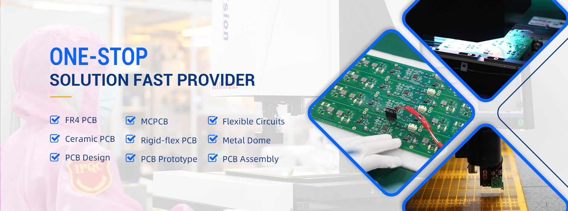
PCB assembly is the process all about putting all the parts you want onto a circuit board. This includes putting on components using different methods like DFA, SMT, and through-hole placements. After everything’s on, it is tested and checked over carefully. To ensure a smooth assembly process, it’s crucial to have a clean list detailing all the necessary parts. Additionally, providing detailed notes on the placement and correct positioning of each part is essential for seamless assembly. These notes should include details like part names, which way they should face, and if they can be washed or not.
Additionally, the technique of joining electrical components to a ceramic printed circuit board is known as Ceramic PCB Assembly. Ceramic printed circuit boards (PCBs) are composed of high-temperature ceramics, including aluminum nitride or alumina.
Ceramic PCB Assembly Process
Surface Preparation
The process starts with careful cleaning. Ceramic PCBs need special cleaning methods to get rid of dirt and make sure solder sticks well. One way to do this is with plasma cleaning. It uses a special kind of gas to clean off any leftover stuff and leave the surface really clean for the next part of the process.
Creating Connections
Once the surface is ready, it’s time to make the electrical paths. Solder paste is a sticky mix of metal powder and flux. It is applied to specific PCB pads by a specialized device known as a stencil printer. This machine controls things like how thick the stencil is, how much pressure to use, and how fast to move the squeegee to make sure the solder paste is applied correctly.
Placing Components
Using specialized machinery, every electrical component from small resistors to complex microchips is precisely positioned on the printed circuit board (PCB). These machines, called pick-and-place machines, are very precise. They make sure each part is fixed where it should, and vision systems make sure the components are facing the right way and that there are no mistakes.
Reflow Soldering
The assembly goes into an oven where the temperature is carefully controlled. As it gets hotter, the solder paste melts, making strong connections between the parts and the PCB. Each type of ceramic needs a different temperature to make sure everything works right and nothing gets harmed.
Inspection and Cleaning
Machines called AOI systems scan for any problems like bad solder, missing parts, or other issues. If anything is wrong, it gets fixed up by hand to make sure everything is perfect and meets the best quality standards.
Functional Verification
The last thing to do is a bunch of tests to check if the PCB works right. We measure things like how much power it uses and if it sends signals the right way. Only if it passes all these tests is the assembly considered finished and ready to be used for what it was made for.
However, the ceramic PCB assembly world has even more to offer. Advanced methods like laser soldering give the accurate results, especially for delicate components. Underfilling is another trick that adds a layer of protection around components, making them safer and better at handling heat. Plus, special cleaning tricks like defluxing get rid of any leftover stuff from soldering, stopping things from rusting and making sure everything lasts a long time.